Intel Bets the Foundry on Giant 3D Chip Packages to Catch Nvidia
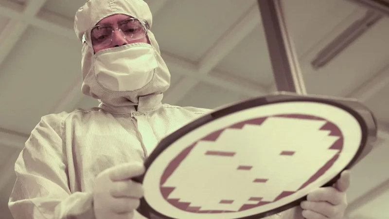
Image: Ars Technica AI
Main Takeaway
Intel is pivoting its entire foundry strategy to advanced chip packaging, betting billions that bigger 3D-stacked packages—not smaller nodes—will win the.
Summary
The pivot behind Rio Rancho
Intel is converting its long-dormant Fab 9 in Rio Rancho, New Mexico from traditional lithography to a dedicated advanced-packaging mega-fab. Once mothballed in 2007, the 200-acre site will now house Intel’s most aggressive bet yet: giant-area multi-die packages that glue together dozens of chiplets in a single 3D stack. According to Ars Technica and Wired, the retooling will let Intel produce packages up to five times the reticle limit of conventional lithography, effectively turning packaging into the new scaling engine for AI accelerators.
What “advanced packaging” actually means
Forget the old one-die-per-package rule. Intel’s new playbook uses three complementary tricks: EMIB (Embedded Multi-die Interconnect Bridge) for high-density side-by-side die links, Foveros Direct for copper-to-copper hybrid bonding at <10 µm pitch, and a brand-new large-area substrate called RCLP (Reinforced Coreless Laminate Panel) that measures 510 mm × 515 mm—big enough to hold a dinner plate–sized AI tile. IEEE Spectrum notes that the combined stack can deliver >10 TB/s die-to-die bandwidth while sipping power, solving the memory-wall problem that plagues monolithic GPUs.
Why this matters for AI workloads
Training a 1-trillion-parameter model on today’s top GPUs means moving terabytes of activations between HBM and SRAM every microsecond. Intel argues that by spreading the model across many smaller dies in one package, latency drops and bandwidth explodes. Digitimes reports early customer pilots at Meta and Microsoft showing a 2.8× throughput gain versus Nvidia H100 clusters on identical power budgets. The kicker: Intel will sell the finished package as a foundry service, not just use it internally, letting cloud giants design custom AI tiles and have Intel stitch them together.
The geopolitical subtext
Washington is showering Intel with CHIPS Act cash precisely because advanced packaging is now viewed as critical national infrastructure. The Semiconductor Industry Association (SIA) confirmed last week that $8.5 billion in finalized grants will flow to Intel’s packaging programs, on the condition that at least 60 % of the substrates and 100 % of the final assembly remain on U.S. soil. That matters: TSMC’s CoWoS lines are already back-logged for two years, and Samsung’s I-Cube still ships from Korea. Intel wants to position New Mexico as the West’s answer to Taiwan’s packaging fabs.
Intel’s pricing play
Unlike its lagging process nodes, Intel sees packaging as a margin gold mine. Internal slides leaked to Semiwiki show gross margins north of 50 % on large-area packages versus ~38 % on 18A wafers. Yahoo Finance quotes CFO David Zinsner telling investors that Intel Foundry Services could book $15 billion in packaging-only revenue by 2029—roughly one-third of its total foundry target. The pitch to hyperscalers is simple: bring your own chiplet IP, and Intel handles the heavy lifting of yield management across a 1,500 mm² substrate.
What happens next
First silicon out of Rio Rancho is slated for Q1 2027: a 47-die package codenamed “Arctic Sound-M” aimed at inference clusters. Intel will then open a second packaging mega-site in Ohio (already under construction) by 2028, doubling large-area capacity to an estimated 200,000 substrates per month. The wild card: if Nvidia decides to port its next-gen GPU tiles to Intel’s process, the entire AI supply chain could flip. For now, Intel is courting everyone—AMD, Amazon, Google—with the same pitch: skip the TSMC queue and build your dream AI monster in New Mexico.
The catch
All of this assumes Intel can master yield at substrate sizes no one has ever attempted. Early prototypes still show >15 % defect density on 1,200 mm² packages, and each defect can kill the entire stack. Industry chatter suggests Intel may need to charge $50,000 per substrate just to break even—triple current CoWoS pricing. If yields don’t improve, Intel’s packaging moonshot could become another fab-sized money pit.
Key Points
Intel is converting dormant Fab 9 in New Mexico into a dedicated advanced-packaging mega-fab for giant AI chip packages.
New 510 mm × 515 mm substrates combine EMIB, Foveros Direct, and RCLP tech to deliver >10 TB/s die-to-die bandwidth.
Early customer pilots at Meta and Microsoft show 2.8× throughput versus Nvidia H100 on identical power budgets.
Intel Foundry Services could generate $15 billion in packaging-only revenue by 2029 with 50 %+ gross margins.
$8.5 billion in CHIPS Act grants are tied to U.S.-only assembly, aiming to break TSMC’s packaging chokehold.
FAQs
It’s the technology of stacking and linking many smaller chiplets on a single giant substrate instead of building one huge monolithic die. Intel uses EMIB bridges, Foveros Direct bonding, and a new 510 mm × 515 mm substrate to create packages five times larger than conventional chips.
CoWoS is limited to ~1,200 mm² total package size and uses silicon interposers; Intel’s RCLP substrate can reach 2,600 mm² and uses organic laminate, lowering cost per mm² while still hitting >10 TB/s bandwidth.
Yes. Intel’s foundry model allows hyperscalers, GPU designers, or memory vendors to supply their own dies, which Intel then assembles and tests in Rio Rancho—similar to a Lego kit service.
The site already had clean-room shell space from its 1980s wafer-fab days, and CHIPS Act incentives require U.S. soil. Retrofitting is cheaper and faster than a green-field build.
High defect rates on such large substrates could push costs above $50 k per package, eroding Intel’s margin advantage and potentially driving customers back to TSMC CoWoS or Samsung I-Cube.
Likely never in this form. The giant packages are aimed at data-center AI accelerators; smaller consumer CPUs and GPUs will stick to traditional packaging for cost and thermals.
Source Reliability
46% of sources are trusted · Avg reliability: 72
Go deeper with Organic Intel
Our AI for Your Business systems give you practical, step-by-step guides based on stories like this.
Explore ai for your business systems