Chip Factories Hit Physical Limits as AI Demand Explodes
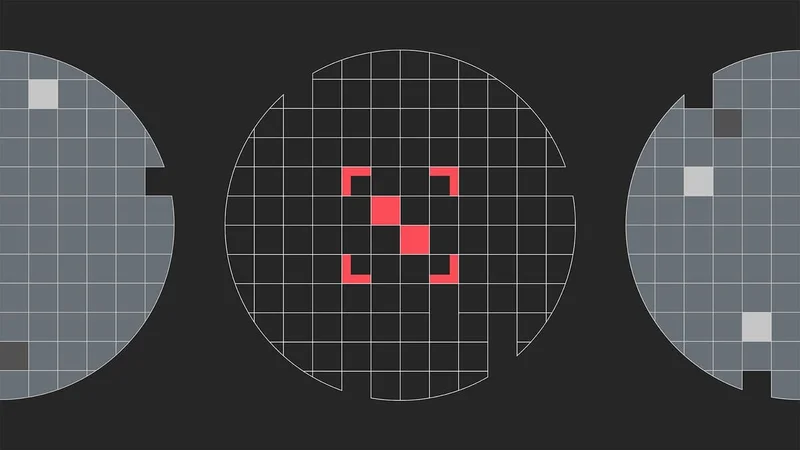
Image: Research.ibm
Main Takeaway
AI workloads are pushing semiconductor manufacturing to breaking point, forcing fabs to rethink design, supply chains, and even physics itself.
Jump to Key PointsSummary
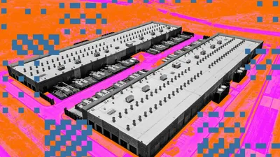
Why fabs are running out of room
AI models now need 10,000x more compute than they did five years ago. That pace is colliding with the physical ceiling of current process nodes. IBM Research warns that at 2 nm and below, every extra transistor adds exponentially more heat and defect risk . McKinsey calls it a "silicon squeeze": demand for GPUs and high-bandwidth memory is growing faster than the industry can add clean-room capacity .
The numbers are stark. Data Bridge Market Research puts the 2032 semiconductor market at over $2 trillion, up from roughly $600 billion today, with AI chips driving the majority of that delta . SEMICON Korea 2026 framed the moment as a "decisive new phase" where the industry must either master sub-nanometer physics or find entirely new architectures .
What this means for developers
If you're building AI products, plan for scarcity. Lead times for NVIDIA H100-class GPUs are already stretching past 52 weeks, and Partanalytics notes that even advanced packaging substrates are on allocation . That means model-training budgets need to lock in hardware contracts 12–18 months ahead of launch, an eternity in startup time.
The shortage is also reshaping software design. Teams are stripping out floating-point precision and leaning on sparsity tricks just to fit models on whatever silicon they can secure. Bloomberg reports that some cloud providers now auction spot GPU time by the minute, pricing that fluctuates like crude oil .
Supply chain rewiring accelerates
Governments are no longer spectators. The CHIPS Act and similar programs in Europe, Japan, and South Korea are pouring roughly $280 billion into new fabs, according to the Semiconductor Industry Association . Bloomberg's video team mapped out a supply chain that once stretched 25,000 miles from sand to server; now it's fragmenting into regional "silicon corridors" to reduce geopolitical risk .
That reshuffle creates new chokepoints. LTTS engineers point out that while new fabs are coming online, the specialized gases, photoresists, and extreme-UV lithography tools still come from a handful of vendors in the Netherlands, Japan, and the U.S. . Any single earthquake or export ban could stall the entire AI build-out.
Manufacturing gets an AI brain of its own
The same models driving demand are being turned inward to fix the problem. IBM is deploying AI vision systems that spot wafer defects down to individual atoms, cutting yield loss by up to 30 % . PDF Solutions claims its AI process-control stack can shave three weeks off a 12-week production cycle by predicting which lots will fail before they reach expensive lithography steps .
McKinsey sees these gains as essential. Without AI-assisted manufacturing, the industry would need to build roughly twice as many fabs to meet 2030 AI demand, an impossible capital lift .
What happens next
The most likely path is a messy hybrid. Near term, expect more multi-die "chiplet" designs that sidestep node limits by spreading workloads across several smaller dies . Medium term, optical interconnects and new memory paradigms (think analog in-memory compute) will start to appear in volume production around 2027–2028. Long term, the industry is already funding research into carbon nanotubes and other post-silicon materials.
For now, every AI roadmap should include a hardware contingency slide. The era of unlimited GPU supply is over, and the companies that secure silicon relationships today will define the next decade of AI capability.
Key Points
AI workloads now require 10,000× more compute than five years ago, hitting physical limits at 2 nm nodes
GPU lead times exceed 52 weeks, forcing developers to pre-book hardware 12-18 months in advance
Global CHIPS Act funding tops $280 billion to regionalize supply chains away from geopolitical risk
IBM and others deploy AI vision systems that cut wafer defects by 30 %, critical for yield at sub-nanometer scales
Market projected to hit $2 trillion by 2032, with AI chips driving majority of growth
Questions Answered
Each leading-edge fab costs $15-20 billion and takes 3-5 years to ramp. Even with $280 billion in government subsidies, equipment bottlenecks for EUV lithography tools limit global capacity to roughly 10 new high-volume fabs per decade.
AI vision systems spot defects at atomic scales, cutting yield loss by 30 %. Predictive models also schedule which wafer lots get priority on expensive lithography steps, trimming 3 weeks off 12-week production cycles.
NVIDIA and cloud providers face immediate revenue risk from allocation limits. TSMC and Samsung bear the capital burden of node shrinks. ASML and Applied Materials control the critical tool supply and can effectively set industry pace.
Chiplet designs spread workloads across smaller dies, optical interconnects reduce power per bit, and research into carbon nanotube transistors and analog in-memory compute offers post-silicon paths for 2030s AI workloads.
Source Reliability
33% of sources are highly trusted · Avg reliability: 62
Go deeper with Organic Intel
Simple AI systems for your life, work, and business. Each one includes copyable prompts, guides, and downloadable resources.
Explore Systems